Transistor Switch Circuits: How to design them
Bipolar junction transistors, BJTs are often used to provide a switching function in a circuit - understand the circuits & how to design them for the best performance.
Transistor Circuit Collection Include:
Transistor circuit collection
Common emitter
Emitter follower
Common base
Darlington pair
Sziklai pair
Current mirror
Long tailed pair
Constant current source
Capacitance multiplier
Two transistor amplifier
High pass filter
Switch circuits
Pulse generator
Schmitt trigger
One transistor relaxation oscillator
Transistor crystal-oscillator
See also:
Transistor circuit design
There are many instances where transistors or to be more specific, bipolar junction transistors, BJTs are used as switches, rather than being used to provide analogue amplification.
Transistor switch circuits are used in many circuit designs and typically need very few electronic components.
These electronic circuit designs may be used to provide higher level switching for integrated circuits where the output drive may not be sufficient. They may be used to provide logic functions in various circuit designs. They may be used to provide a switching capability for many circuits - they may even be used to drive some form of electromechanical relay.
Transistor switch basics
Transistors are able to be used as switches. The original way of using a transistor was in an analogue mode where the level of the output varies over a range in line with the input.
However it is also possible to use it so that it either conducts fully, or does not conduct at all. To achieve this, there are two conditions. Either no current is passed into the base, so that it does not conduct and it can be considered to be OFF, or sufficient current can be passed into the base so that it fully conducts and it can be considered to be ON.

For switching, the transistor is generally operated in the common emitter mode, with drive being applied to the base and the collector emitter circuit being switched ON and OFF.
The essence, not surprisingly, about using a transistor as a switch is that it operates in one of either two states: ON or OFF. It is never between the two, apart from when it transitions, and this is achieved as quickly as possible.
In the fully ON state the transistor does have a small voltage between the collector and emitter. This is known as the collector emitter saturation voltage VCEsat and it is quoted in the data-sheets for transistors.

The saturation voltage occurs when the transistor is unable to pass any more current, and there is a residual voltage across the transistor. This saturation voltage is typically around 0.5 to 0.2V, although my experience is that it tends to be more towards the 0.2V figure for most cases.
When designing a transistor switch circuit, the base must be driven sufficiently hard to ensure that it will saturate, but not too much otherwise too much charge will be stored and it will take longer for the transistor to switch off.
Other factors to consider are the maximum collector current. The maximum that should be switched should fall well within this limit, typically around 60% of the maximum rating is good.
Also it is necessary to consider the minimum hFE as this will determine the drive required for the base.
The voltage specifications can also be important, but if the circuit is to be used with low voltages, this is typically not a major issue.
It is worth noting the polarity of the signal for this circuit. When the input voltage is high, current will flow into the base of the transistor and turn the transistor ON. This will mean that current will flow through the load, but the voltage at the output will be the inversion of the input.
This can be used to turn a relay on, a diode or incandescent light, etc. For these, when the input is high, the load will be passing current and the relay, lamp, etc will be on.

Note that for this circuit, the input voltage to switch the transistor ON, does not need to be the same as the rail voltage. For example, a 5 volt logic signal could be used to turn the transistor ON, but the transistor supply rail could be +12 or +15 volts, etc.
Transistor switch electronic circuit design process
When designing a basic one transistor switch circuit, there are several steps within the overall design process that need to be undertaken.
Understand the requirements: The first stage is to understand the requirements, and note the input drive that can be provided as well as the output current and voltage swing that is necessary.
Select transistor type: The next step is the selection of the transistor. This might normally be an NPN type as most rails are negative and the ground line is positive. The transistor should have a current gain that will be able to provide sufficient current at the output from the current available from the previous stage.
Calculate the load resistor required for the output: This will be governed by the current required to flow in the collector circuit.
Note that if an LED indicator is to be driven in this circuit design, then this will drop about 1.2 volts or thereabouts and this will need to be included. In other words the equation will need to be modified so that the voltage on the top line is (VCC -VCEsat - VLED). Where VLED) is the voltage dropped across the LED.
Calculate base current required: The calculation for the base current is easily calculated by dividing the collector current by the current gain of the transistor. As the current gain of bipolar transistors varies considerably between one device and the next, it is important to take the lowest value that might be encountered as you can never know what the performance of the particular transistor used might be.
It is worth checking at this stage whether the driver stage can supply the required level of current.
Calculate base series resistor: The calculation of the resistor is achieved by simply using Ohm's Law.
To calculate this, take the lowest value of voltage from the previous stage, remembering it could fall when supplying current. Subtract from this the base emitter voltage of the BJT switch device - 0.7 volts for silicon. This is then divided by the current previously calculated to give the required resistor value. Take the nearest preferred value possibly erring on the side of the lower resistor to make sure that sufficient current is provided.
Base leakage resistor: In order to ensure the fastest switching, and also ensure any base leakage does not cause the base to float high in voltage, a resistor between the base and ground is often incorporated. Typically this could be around five to ten times that of the series base resistor - its value is not critical, but it can improve the switching performance. With values around ten times that of the series resistor, and if a generous level of base current is provided, then little or no adjustment needs to be made to the series resistor value.
With all these stages completed, the BJT switch circuit design is complete. It is very straightforward because the circuit itself is not complicated.
Alternative transistor switch circuits
Although the most common type of circuit is the NPN common emitter circuit that we've discussed, there are other electronic circuit designs that can be used to provide different switching scenarios.
The basic common emitter circuit has the load between the supply rail and the transistor collector. In some instances it is necessary to have one side of the load connected to ground.
It is very easy to switch the polarity of the transistor to a PNP type and operate the circuit with one side of the load grounded.

Again, a simple series resistor is needed, but this time remember that when the input is drawn low, i.e. near to zero volts, then current will flow through the load, i.e. the circuit will be ON.
When using this circuit, it is worth remembering the sense of the switching. When the input is pulled high, then the transistor is turned off and current through the load is zero.
It is also necessary to remember that for the transistor to turn OFF, the input voltage must be drawn up to the rail voltage. This might not be an issue for some circuit designs, but especially where the input control voltage may not be guaranteed to reach the rail voltage this is an issue. Even TTL logic that runs on 5 volt rails, the HIGH output could be as low as 2.4 volts and this would not guarantee the transistor turning OFF if it ran from a 5 volt rail.
In other words the disadvantage of this circuit is that the control voltage needs to change from the rail voltage to a low state sufficient to turn the transistor ON. This may not always be easy to achieve.
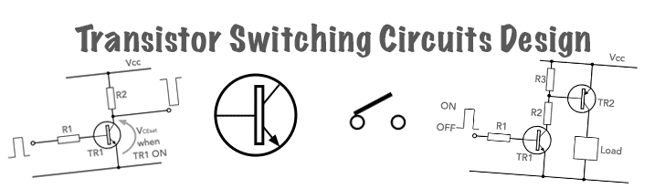
To overcome this problem, is very easy. It is possible to add a driver transistor before the final switching one.

In this circuit the first transistor is an NPN transistor and it acts as a single transistor switch, turning ON and OFF according to the input control voltage. When TR1 is OFF, its collector will reach the rail voltage and this will enable it to turn the second PNP transistor fully OFF.
When the control voltage is high, this will turn TR1 ON, which will pull its collector to near 0V, i.e. VCEsat above 0V and this will mean that the base of TR2 draws current and will in turn draw current through its load as the collector of TR2 will be VCEsat below the rail voltage.
The potential divider formed from the two resistors in the collector circuit of TR1, i.e. R2 and R3 ensure the correct operation of TR2. The purpose of R3 is to ensure that TR2 remains OFF when this is required.
R3 ensures that the base of TR2 remains high when TR1 is OFF and this ensures that the voltage on the base of TR2 remains high to ensure a proper switching state.
Top tips for transistor switch circuit designs
Transistor switching circuits are typically very easy to design, but sometimes a few precautions need to be observed if the circuit is to work effectively and reliably.
The pointers or hints and tips below have been learned the hard way and may well help in ensuring the circuit operates as planned.
Use a switching transistor: When fast speeds are required a switching transistor should be used as this will have fast switching times and low levels of charge storage within the device. I can remember using an RF transistor with a very high fT transition frequency which was well above the speed required for the pulse being presented to the transistor, but nothing was seen on the output. Only when charging to a switching transistor was the problem resolved.
Use a base leak resistor: Although a base leak resistor is not essential in many circuit designs, incorporating one will ensure that the transistor base has a leakage path to ground and therefore it will not float up in voltage and provide spurious turn on instances. IT will also help improve the switching speed as charge can pass to ground as the input voltage falls.
Provide sufficient base drive, but not too much: There should be sufficient drive current to ensure that the transistor turns on properly for all levels of transistor gain, but don't overdrive as this can reduce the switching speed - this can be important in some logic circuits where speed may be a key parameter.
It is important to remember that the transistor current gain will have a wide variation, but will be defined in the data-sheet. Also the gain will drop with temperature, so if the circuit is to be used in low ambient temperatures, then this needs to be accommodated.
Remember a protective diode for inductive loads: If the transistor is to drive an inductive load such as a reed relay, etc, then a diode should be placed across the load to prevent back EMF from destroying the transistor as it turns off.

Transistor switch circuit with protection diode for inductive load Under normal operating conditions the diode is reverse biassed, but when the transistor turns off, a back EMF is produced, but when this happens the diode goes into forward conduction and absorbs any spikes that could damage the circuitry.
Remember a transistor switch will never be as fast as the output from a logic IC: It is important to remember that a transistor switching circuit will never be as fast as the output from a logic IC. This is because the logic ICs have very small internal dimensions and the circuits are optimised for speed. One transistor circuits like those shown are much larger and will suffer from much higher levels of spurious capacitance and inductance which will slow the output. Also, they will not use the complementary symmetry output configurations of the IC that enable their very high speeds to be achieved.
Remember the sense of the switching: It is important to remember the sense of the circuit, i.e. whether the output is On or OFF for a particular input state. Although the voltage of the simple common emitter switch si such that when the voltage on the input is HIGH and causes current to flow in the base so that the output conducts and the voltage falls to the LOW state, the fact that the transistor output is LOW means that current is flowing and the indicator, relay, etc will have current flowing and may be considered to be ON. Also for other configurations, there are inversions, so beware.
These are just a few circuit design tips that could be useful when designing a switching circuit using a bipolar junction transistor, BJT.
There are very many different electronic circuit designs in which transistors are used as the basic building block. Switching circuits are just one: where the drive capability of the previous stage is insufficient to give the level of drive capability required.
More Circuits & Circuit Design:
Op Amp basics
Op Amp circuits
Power supply circuits
Transistor design
Transistor Darlington
Transistor circuits
FET circuits
Circuit symbols
Return to Circuit Design menu . . .