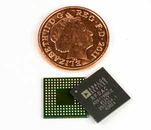
Ball Grid Array, BGA
SMD ball grid array, BGA packages enable high density connections to be made more easily to integrated circuits by allowing the under-side of a chip package to be used for the connectivity.
Surface Mount Technology, SMT Includes:
What is SMT
SMD packages
Quad flat pack, QFP
Ball grid array, BGA
Plastic leaded chip carrier, PLCC
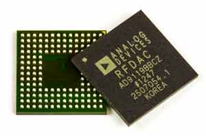
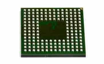
The Ball Grid Array has become increasingly popular for SMD ICs that require high density connections. Using the under-side of the IC package rather than connections around the edge, this enables connection density of be reduced, simplifying PCB layout.
The main problem with using SMD BGA IC packages is that using the under-side of the chip means that direct access to the connections is not possible, making soldering, de-soldering and inspection more difficult. However with mainline PCB production equipment, these issues are easy to overcome and the overall reliability and performance can be improved.
Rationale for BGA usage
There have rationale for the introduction and use of the ball grid arraye, BGA is quite straightforward as there had been issues with other technologies. The conventional quad flat pack style packages had very thin and very closely spaced pins. This configuration gives rise to a number of difficulties.
- Damage: The pins on QFPs are naturally very thin and their spacing means that their position needs to be controlled very closely. Any mishandling can lead to them being displaced and when this happens they are almost impossible to restore. ICs using high pin counts tend to be very expensive, so this can become a major issue.
- Pin density: From a design viewpoint, the pin density was such that taking the tracks away from the IC also proved to be problematic as there could be congestion in some areas.
- Soldering process In view of the very close spacing of the QFP pins, very careful control of the soldering process is required otherwise contacts can be easily bridged.
The BGA package was developed to overcome these problems, and improve reliability from the soldered joints. As a result the BGA is widely used and processes and equipment have been developed to overcome the problems with their use.
Ball Grid Array BGA aims
The Ball Grid Array was developed to provide a number of benefits to IC and equipment manufacturers as well as providing benefits to the eventual users of equipment. Some of the BGA benefits over other technologies include:
- Efficient use of printed circuit board space, allowing connections to be made under the SMD package and not just around its periphery
- Improvements in both thermal and electrical performance. BGA packages can offer power and ground planes for low inductances and controlled impedance traces for signals as well as being able to route heat away via the pads, etc.
- Improvements in manufacturing yields as a result of the improved soldering. BGAs allow wide spacing between connections as well as a better level of solderability.
- Reduced package thickness which is a great advantage when many assemblies need to be made much thinner, e.g. mobile phones, etc.
- Improved re-workability resulting from larger pad sizes, etc.
These advantages have meant that despite initial scepticism about the package, it provides some useful improvements in many circumstances..
What is a BGA package?
The Ball Grid Array, BGA, uses a different approach to the connections to that used for more conventional surface mount connections. Other packages such as the quad flat pack, QFP, used the sides of the package for the connections. This meant that there was limited space for the pins which had to be spaced very closely and made much smaller to provide the required level of connectivity. The Ball Grid Array, BGA, uses the underside of the package, where there is a considerable area for the connections.
The pins are placed in a grid pattern (hence the name Ball Grid Array) on the under-surface of the chip carrier. Also rather than having pins to provide the connectivity, pads with balls of solder are used as the method of connection. On the printed circuit board, PCB, onto which the BGA device is to be fitted there is a matching set of copper pads to provide the required connectivity.
Apart from the improvement in connectivity, BGAs have other advantages. They offer a lower thermal resistance between the silicon chip itself than quad flat pack devices. This allows heat generated by the integrated circuit inside the package to be conducted out of the device onto the PCB faster and more effectively. In this way it is possible for BGA devices to generate more heat without the need for special cooling measures.
In addition to this the fact that the conductors are on the underside of the chip carrier means that the leads within the chip are shorter. Accordingly unwanted lead inductance levels are lower, and in this way, Ball Grid Array devices are able to offer a higher level of performance than their QFP counterparts.
BGA package types
In order to meet the variety of requirements for different types of assembly and equipment, a number of BGA variants have been developed.
- MAPBGA - Moulded Array Process Ball Grid Array: This BGA package is aimed at low-performance to mid-performance devices that require packaging with low inductance, ease of surface mounting. It provides a low cost option with a small footprint and high level of reliability.
- PBGA - Plastic Ball Grid Array: This BGA package is intended for mid- to high-performance devices that require low inductance, ease of surface mounting, relatively low cost, while also retaining high levels of reliability. It has some additional copper layers in the substrate that enable increased power dissipation levels to be handled.
- TEPBGA - Thermally Enhanced Plastic Ball Grid Array: This package provides for much higher heat dissipation levels. It uses thick copper planes in the substrate to draw heat from the die to the customer board.
- TBGA - Tape Ball Grid Array: This BGA package is a mid- to high-end solution for applications needing high thermal performance without an external heatsink.
- PoP - Package on Package: This package may be used in applications where space is at a real premium. It allows for stacking a memory package on top of a base device.
- MicroBGA: As the name indicates this type of BGA package is smaller than the standard BGA package. There are three pitches that are prevalent in the industry: 0.65, 0.75 and 0.8mm.
BGA assembly
When BGAs were first introduced, BGA assembly was one of the key concerns. With the pads not accessible in the normal manner would BGA assembly reach the standards that could be achieved by more traditional SMT packages. In fact, although soldering may have appeared to be a problem for a Ball Grid Array, BGA, device, it was found that standard reflow methods were very suitable for these devices and joint reliability was very good. Since then BGA assembly methods have improved, and it is generally found that BGA soldering is particularly reliable.
In the soldering process, the overall assembly is then heated. The solder balls have a very carefully controlled amount of solder, and when heated in the soldering process, the solder melts. Surface tension causes the molten solder to hold the package in the correct alignment with the circuit board, while the solder cools and solidifies. The composition of the solder alloy and the soldering temperature are carefully chosen so that the solder does not completely melt, but stays semi-liquid, allowing each ball to stay separate from its neighbours.
As many products now utilise BGA packages as standard, BGA assembly methods are now well established and can be accommodated by most manufacturers with ease. Accordingly there should be no concerns about using BGA devices in a design.
Ball Grid Array, BGA, inspection
One of the problems with BGA devices is that it is not possible to view the soldered connections using optical methods. As a result there was some suspicion about the technology when it was first introduced and many manufacturers undertook tests to ensure that they were able to solder the devices satisfactorily. The main problem with soldering Ball Grid Array devices, is that sufficient heat must be applied to ensure that all the balls in the grid melt sufficiently for every joint to be satisfactorily made.
The joints cannot be tested fully by checking the electrical performance. It is possible that the joint may not be adequately made and that over time it will fail. The only satisfactory means of inspection is to use X-ray inspection as this means of inspection is able to look through the device at the soldered joint beneath.It is found that once the heat profile for the solder machine is set up correctly, the BGA devices solder very well and few problems are encountered, thereby making BGA assembly possible for most applications.
Ball Grid Array, BGA rework
As might be anticipated, it is not easy to rework boards containing BGAs unless the correct equipment is available. If a BGA is suspected as being faulty, then it is possible to remove the device. This is achieved by locally heating the device to melt the solder underneath it.
In the BGA rework process, the heating is often achieved removed in a specialised rework station. This comprises a jig fitted with infrared heater, a thermocouple to monitor the temperature and a vacuum device for lifting the package. Great care is needed to ensure that only the BGA is heated and removed. Other devices nearby need to be affected as little as possible otherwise they may be damaged.
BGA repair / BGA reballing
Once removed, the BGA can be replaced with a new one. Occasionally it may be possible to refurbish or repair a BGA that has been removed. This BGA repair may be an attractive proposition if the chip is expensive and it is known to be a working device once removed. Undertake a BGA repair it needs to have the solder balls replaced in a process known as reballing. This BGA repair can be undertaken using some of the small ready-made solder balls that are manufactured and sold for this purpose.
There are many organisations that have been set up with specialist equipment to undertake this BGA reballing.
BGA, ball grid array technology has become well established. Although it might appear that there would be issues with lack of access to the contacts, suitable methods of overcoming these have been found. PCB layout and board reliability have been improved as track and pin density has reduced, and in addition to this soldering has become more reliable and infra-red reflow techniques have been refined to enable reliable soldering. Similarly inspection of boards using BGAs can use X-ray inspection, AXI, and in addition to this rework techniques have been developed. As a result the use of BGA technology has lead to an overall improvement in quality and reliability.
More Electronic Components:
Batteries
Capacitors
Connectors
Diodes
FET
Inductors
Memory types
Phototransistor
Quartz crystals
Relays
Resistors
RF connectors
Switches
Surface mount technology
Thyristor
Transformers
Transistor
Unijunction
Valves / Tubes
Return to Components menu . . .