What is a Phototransistor: tutorial & primer
Phototransistors are a form of bipolar transistor that is sensitive to light - having the gain of a transistor they are much more sensitive than photodiodes and find uses in many light detection circuit designs.
Phototransistor Includes:
Phototransistor basics
Applications & circuits
Photodarlington
Optocoupler / optoisolator
The phototransistor is a semiconductor device that is able to sense light levels and alter the current flowing between emitter and collector according to the level of light it receives.
Phototransistors and photodiodes can both be used for sensing light, but the phototransistor is more sensitive in view of the gain provided by the fact that it is a bipolar transistor. This makes phototransistors more suitable in a number of applications.
Although all bipolar transistors themselves are light sensitive, which is why most transistors are encapsulated in metal or plastic cans, phototransistors are a specialised form of bipolar transistor that have been optimised for its light sensitivity, making these electronic components ideal for many light sensing applications.
.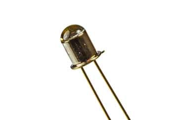
Note the lens at the top and the fact that it only has two leads because the base is often left open circuit and no external connection is provided.
The idea of the phototransistor has been known for many years. William Shockley first proposed the idea in 1951, not long after the ordinary bipolar transistor had been discovered. It was then only two years before the photo-transistor was demonstrated.
Since their first introduction and use, phototransistors have been used in a variety of circuit designs and applications, and their development has continued ever since.
Phototransistors are widely available and can easily be obtained quite cheaply from electronic component distributors - in view of their use in many electronic circuits and applications, they are available as part of the standard semiconductor device inventory.
In view of the fact that these electronic components are cheap and easily available, it is necessary to ensure that the selected component meets the requirements of the circuit design in which it will be used. Understanding the various specifications is important for this.
Initial development of the phototransistor
The phototransistor invention followed on from the development of the first point contact transistor. A large number of semiconductor developments were being undertaken at Bell Labs around this time, and the phototransistor was development by one of the teams there.
Although the history of the phototransistor is not as well publicised as many of the other early semiconductor developments, it was certainly a very important development.
Note on the Phototransistor History:
The phototransistor came out of the early semiconductor developments that took place at Bell Telephone Laboratories. The invention was first announced on 30th March 1950.
Read more about Phototransistor Invention
Phototransistor operation
The phototransistor uses the basic bipolar transistor concept as the basis of its operation. In fact a phototransistor can be made by exposing the semiconductor of an ordinary transistor to light. Very early photo transistors were made by not covering the plastic encapsulation of the bipolar transistor with black paint.
The photo-transistor operates because light striking the semiconductor frees electrons / holes and causes current to flow in the base region.
Photo-transistors are operated in their active regime, although the base connection is generally left open circuit or disconnected because it is often not required. The base of the photo transistor would only be used to bias the transistor so that additional collector current was flowing and this would mask any current flowing as a result of the photo-action. For operation the bias conditions are quite simple. The collector of an NPN transistor is made positive with respect to the emitter or negative for a PNP transistor.
The light enters the base region where it causes hole electron pairs to be generated. This generation mainly occurs in the reverse biased base-collector junction. The hole-electron pairs move under the influence of the electric field and provide the base current, causing electrons to be injected into the emitter. As a result the photodiode current is multiplied by the current gain β of the transistor.
The performance of the phototransistor can be superior to that of the photodiode for some applications in view of its gain. As a rough guide, where a photodiode may enable a current flow of around 1µA under typical room conditions, a phototransistor may allow a current of 100µA to flow. These are very rough approximations, but show the order of magnitude of the various values and comparisons.
One of the drawbacks of the phototransistor is that is particularly slow and its high frequency response is very poor. Photo-diodes are much faster electronic components and are used where speed is essential despite their inferior sensitivity.
Phototransistor circuit symbol
Standard circuit symbols are essential for each type of electronic component, enabling circuit diagrams to be drawn easily and recognisable by all. The phototransistor symbol consists of the basic bipolar transistor symbol with two arrows pointing towards the junction of the bipolar transistor. This diagrammatically represents the operation of the phototransistor.

Phototransistors can be based around both NPN transistors and PNP transistors and therefore it is perfectly possible to have a PNP phototransistor, and for this the direction of the arrow on the emitter is reversed in the normal way.
It can be seen that the phototransistor symbol shown does not give a base connection. Often the base is left disconnected as the light is used to enable the current flow through the phototransistor. In some instances the base may be biased to set the required operating point. In this case the base will be shown in the normal way on the phototransistor symbol.
Phototransistor structure
Although ordinary bipolar transistors exhibit the photosensitive effects if they are exposed to light, the structure of the phototransistor is specifically optimised for photo applications. The photo transistor has much larger base and collector areas than would be used for a normal transistor. These devices were generally made using diffusion or ion implantation.

Early photo transistors used germanium or silicon throughout the device giving a homo-junction structure. The more modern phototransistors use type III-V semiconductor materials such as gallium arsenide and the like. NPN transistor varieties are more popular in view of the fact that negative ground systems are used, and NPN transistors fit this mode of operation better.
Heterostructures that use different materials either side of the PN junction are also popular because they provide a high conversion efficiency. These are generally fabricated using epitaxial growth of materials that have matching lattice structures.
These photo transistors generally use a mesa structure. Sometimes a Schottky (metal semiconductor) junction can be used for the collector within a phototransistor, although this practice is less common these days because other structures offer better levels of performance.
In order to ensure the optimum conversion and hence sensitivity, the emitter contact is often offset within the phototransistor structure. This ensures that the maximum amount of light reaches the active region within the phototransistor.
Phototransistor characteristics
As already mentioned the photo-transistor has a high level of gain resulting from the transistor action. For homo-structures, i.e. ones using the same material throughout the semiconductor device, this may be of the order of about 50 up to a few hundred.
However for the hetero-structure devices, the levels of gain may rise to ten thousand. Despite their high level of gain the hetero-structure devices are not widely used because these semiconductor devices are considerably more costly to manufacture. A further advantage of all phototransistors when compared to the avalanche photodiode, another device that offers gain, is that the phototransistor has a much lower level of noise. Avalanche diodes of all forms are known for the large levels of noise they generate as a result of the avalanche process.
One of the main disadvantages of the phototransistor is the fact that it does not have a particularly good high frequency response. This arises from the large capacitance associated with the base-collector junction. This junction is designed to be relatively large to enable it to pick up sufficient quantities of light. For a typical homo-structure device the bandwidth may be limited to about 250 kHz. Hetero-junction devices have a much higher limit and some can be operated at frequencies as high as 1 GHz.
The characteristics of the photo-transistor under different light intensities. They are very similar to the characteristics of a conventional bipolar transistor, but with the different levels of base current replaced by the different levels of light intensity.
There is a small amount of current that flows in the photo-transistor even when no light is present. This is called the dark current, and represents the small number of carriers that are injected into the emitter. Like the photo-generated carriers this is also subject to the amplification by the transistor action.
Phototransistor applications
The fact that phototransistors are easy to use and perform well, within their limitations, means that these semiconductor devices are used in a wide variety of electronic circuit designs.
Often the circuits and applications are where a light beam is interrupted, but sometimes they can be used for light level detection.
- Encoders where a rotating disc with light and dark stripes rotates - this gives speed and direction or rotation.
- Card readers.
- Security systems
- Infra-red detectors.
- Lighting control.
- Opto-couplers
- Counting systems - a light or IR beam is interrupted for each item counted.
- Lighting control.
There are of course, many other applications where these electronic components are used.
Summary of advantages and disadvantages of phototransistors
Although these semiconductor devices are used in a huge number of electronic devices, circuits and applications, their advantages and disadvantages need to be weighed up to determine whether they are the right electronic component for the given application. Photoresistors or light dependent resistors LDRs; photodiodes; photodarlingtons, photo-FETs and even photo-thyristors and triacs are all available and may suit any given application.
Phototransistor advantages
- Have a relatively high gain and therefore they are relatively sensitive.
- These electronic components are relatively cheap as they are effectively a transistor that is open to light.
- They can be incorporated into an integrated circuit.
- Offer a reasonable speed.
Phototransistor disadvantages
- These devices cannot handle the high voltages of other semiconductor devices like photo-thyristors and triacs.
- In applications where they are exposed to transient voltage spikes and surges, they are open to damage
- Not as fast as other light sensitive electronic components like photo-diodes.
These are some of the main advantages and disadvantages for these electronic components.
Phototransistors are semiconductor devices based around the basic bipolar transistor, and they are available as NPN transistors or PNP transistors. Along with other electronic components and semiconductor devices they are available from virtually all electronic component distributors and often their cost is very low.
More Electronic Components:
Batteries
Capacitors
Connectors
Diodes
FET
Inductors
Memory types
Phototransistor
Quartz crystals
Relays
Resistors
RF connectors
Switches
Surface mount technology
Thyristor
Transformers
Transistor
Unijunction
Valves / Tubes
Return to Components menu . . .