MOSFET - Metal Oxide Semiconductor Field Effect Transistor
The MOSFET, Metal Oxide Semiconductor Field Effect Transistor or FET has an oxide film between the gate and the channel to increase the input impedance and reduce the overall circuit current.
FETs, Field Effect Transistors Includes:
FET basics
FET specifications
JFET
MOSFET
Dual gate MOSFET
Power MOSFET
MESFET / GaAs FET
HEMT & PHEMT
FinFET technology
IGBT
Silicon carbide, SiC MOSFET
GaN FET / HEMT
The MOSFET or metal oxide semiconductor field effect transistor, is a form of FET that offers an exceedingly high input impedance.
The gate input has an oxide layer insulating it from the channel and as a result its input resistance is very many MΩ.
The MOSFET has a number of different characteristics compared to the junction FET, and as a result it can be used in a number of different areas and it is able to provide excellent performance.
One particular area where MOSFET technology is used is within CMOS logic integrated circuits. The extraordinarily high input impedance means that these circuits are able to consume very low power levels and this means that high levels of integration can be achieved.
MOSFET development
The concept of the MOSFET has been known for many years but they only became important in mid to late 1960s.
One of the major problems experienced with the early development of MOSFETs was associated in developing the insulating oxide layers. The problems were only overcome as the semiconductor materials and processing technology improved. As a result, in the late 1960s MOSFET technology became more widespread.
Now MOSFET technology is one of the most widely used semiconductor techniques, having become one of the principle elements in integrated circuit technology.
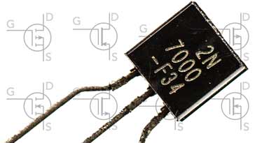
MOSFET circuit symbol
There is a variety of different circuit symbols used for MOSFETs. In view of the different variety of standards used, along with the different types of MOSFET, a host of different MOSFET circuit symbols can be seen.

MOSFET circuit symbol notes:
- The circuit symbol for the basic MOSFET (shown left most) indicates that the device has a bulk substrate - this is indicated by the arrow on the central area of the substrate.
- The MOSFET circuit symbols shown in the centre and marked "enhancement no bulk semi" are both valid and used equally frequently. They indicate an enhancement MOSFET that has no bulk semiconductor.
- Depletion mode MOSFETs are generally indicated as shown on the right most section.
MOSFET circuit symbols for both P-channel and N-channel types are shwn. The drain is shown at the top as this is generally as they are seen on circuit diagrams.
MOSFET key parameters
Before looking at the operation of the MOSFET, it is worth summarising a few of the key features associated with MOSFET technology.
| Key MOSFET Features | |
|---|---|
| Feature | Details |
| Gate construction | The gate is physically insulated from the channel by an oxide layer. Voltages applied to the gate control the conductivity of the channel as a result of the electric field induced capacitively across the insulating dielectric layer. |
| N / P channel | Both N-channel and P-channel variants are available |
| Enhancement / depletion | Both enhancement and depletion types are available. As the name suggests the depletion mode MOSFET acts by depleting or removing the current carriers from the channel, whereas the enhancement type increases the number of carriers according to the gate voltage. |
MOSFETs may be characterised as N Channel and P-Channel. Each has different characteristics:
| Comparison of the key features of N-channel and P-channel MOSFETs | ||
|---|---|---|
| Parameter | N-channel | P-channel |
| Source / drain material | N-Type | P-Type |
| Channel material | P-Type | N-Type |
| Threshold voltage Vth | negative | doping dependent |
| Substrate material | P-Type | P-Type |
| Inversion layer carriers | Electrons | Holes |
MOSFET operation: how a MOSFET works
Like other forms of FET, the current flowing in the channel of the MOSFET is controlled by the voltage present on the gate. As such MOSFETs are widely used in applications such as switches and also amplifiers. They are also able to consume very low levels of current and as a result they are widely used in microprocessors, logic integrated circuits and the like. CMOS integrated circuits used MOSFET technology.
Note: In view of the structure of the MOSFET - its gate is insulated from the channel by a thin oxide layer and this means that it can be damaged by static if it is not handled in the correct way, or the circuit does not protect it adequately.
Also like other forms of FET, the MOSFET is available in depletion mode and enhancement mode variants. The enhancement mode is what may be termed normally OFF, i..e when the VGS gate source voltage is zero and requires a gate voltage to turn it on, whereas the other form, deletion mode devices are normally ON when VGS is zero.
There are basically three regions in which MOSFETs can operate:
- Cut-off region: In this region of the MOSFET is in a non-conducting state, i.e. turned OFF - channel current IDS = 0. The gate voltage VGS is less than the threshold voltage required for conduction.
- Linear region: In this linear region the channel is conducting and controlled by the gate voltage. For the MOSFET to be in this state the VGS must be greater than the threshold voltage and also the voltage across the channel, VDS must be greater than VGS.
- Saturation region: In this region the MOSFET is turned hard on. The voltage drop for a MOSFET is typically lower than that of a bipolar transistor and as a result power MOSFETs are widely used for switching large currents.
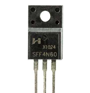
A power MOSFET in a TO220 package Switching for Different Types of MOSFET MOSFET type VGS +ve VGS 0 VGS -ve N-Channel Enhancement ON OFF OFF N-Channel Depletion ON ON OFF P-Channel Enhancement OFF OFF ON P-Channel Depletion OFF ON ON
MOSFET structure
As already implied the key factor of the MOSFET is the fact that the gate is insulated from the channel by a thin oxide layer. This forms one of the key elements of its structure.
For an N-channel device the current flow is carried by electrons and in the diagram below it can be seen that the drain and source are formed using N+ regions which provide good conductivity for these regions.
In some structures the N+ regions are formed using ion implantation after the gate area has been formed. In this way, they are self-aligned to the gate.
The gate to source and gate to drain overlap are required to ensure there is a continuous channel. Also the device is often symmetrical and therefore source and drain can be interchanged. On some higher power designs this may not always be the case.

It can be seen from the diagram that the substrate is the opposite type to the channel, i.e. P-type rather than N-type, etc. This is done to achieve source and drain isolation.
The oxide over the channel is normally grown thermally as this ensure good interfacing with the substrate and the most common gate material is polysilicon, although some metals and silicides can be used.
The depletion mode has a slightly different structure. For this a separate N-type channel is set up within the substrate.

P-channel FETs are not as widely used. The main reason for this is that the holes do not have as high a level of mobility as electrons, and therefore the performance is not as high. However they are often required for use in complementary circuits, and it is mainly for this reason that they are manufactured or incorporated into ICs.
MOSFETs are possibly the most widely used active device. As they appear in CMOS and other integrated circuit technologies where they enable very low power operation - a requirement for very large scale integration, otherwise power consumption would be far too high.
Not only are they used in IC technology, but they are also used as discrete components as well where they are able to offer very high input impedance levels and also low noise operation in oscillators, amplifiers and many other circuits.
More Electronic Components:
Batteries
Capacitors
Connectors
Diodes
FET
Inductors
Memory types
Phototransistor
Quartz crystals
Relays
Resistors
RF connectors
Switches
Surface mount technology
Thyristor
Transformers
Transistor
Unijunction
Valves / Tubes
Return to Components menu . . .