What is Electrostatic Discharge: ESD basics
- a tutorial, overview or summary of the basics of Electrostatic Discharge, ESD and how to avoid its effects on electronics components.
Home » Construction & manufacture » this page
ESD Tutorial Includes:
ESD Basics
How ESD affects electronics components
Protecting against ESD
ESD protected area
ESD workbench
ESD work mat
ESD wrist strap
ESD clothing
ESD storage
ESD process
ESD on a budget
Design to combat ESD
Electrostatic Discharge or ESD is a fact of everyday life and it is of particular importance in the electronics industry these days.
Years ago when thermionic valves / vacuum tubes were used it was not a problem, and even with the introduction of transistors few considered it a problem. However when MOSFETs were introduced their failure rates rose, the problem was investigated and it was found that static build up was sufficient to cause the oxide layer in the device to fail.
Since then the awareness of ESD has risen considerably because it has been shown to have an effect on many devices. In fact many manufacturers today consider all components to be static sensitive, not just MOS devices that are the most prone to damage.
As a result of the importance attached to ESD manufacturers of electronics equipment spend many thousands of pounds to ensure their workplaces are protected against the effects of static. They ensure that the products they manufacture do not have high failure rates during manufacturing test, and are able to demonstrate a high reliability over a long period of time.
What is ESD?
Static is simply the build up of charge between two surfaces. It arises when surfaces rub together and this results in an excess of electrons on one surface and a deficiency on the other.
The surfaces on which the charge builds up may be considered as a capacitor. The charge will remain in place unless it has a path through which it can flow. As there is often no real path through which the charge can flow the resultant voltage may remain in place for some time and this gives rise to the term "static electricity".
However when a conduction path does exist a current will flow and the charge will be reduced. There is a time constant associated with the discharge. A high resistance will mean that a smaller current will flow for a longer time. A low resistance will give rise to a much faster discharge.
Obviously the levels of voltage and current which are produced depend of a large variety of factors. The size of the person, the level of activity, the object against which the discharge is made, and of course the humidity of the air. These all have a pronounced effect so it is almost impossible to predict the exact size of the discharges that will occur.
However one of the major factors that affects the voltages that are produced is the types of material that are being rubbed together. It is found that different materials give different voltages. The voltage produced is dependent upon the position of the two materials in a series known as the tribo-electric series.
Tribo-electric series
The further apart they are in the series, the greater the voltage. The one that is higher up the series will receive a positive charge, and the one lower down a negative charge. Looking at the tribo-electric series list below it can see that combing ones hair with a plastic comb will give rise to a positive charge on the hair, and the comb will become negatively charged.
Positive charge
Skin
Hair
Wool
Silk
Paper
Cotton
Wood
Rubber
Rayon
Polyester
Polythene
Pvc
Teflon
Negative charge
There are many ways in which charges can be built up. Even walking across a carpet can give rise to some very large voltages. Typically this might give rise to potentials of 10 kV. In bad cases it could even lead to potentials of three times this value. Even the act of walking across a vinyl floor may lead to potentials of around 5 kV being generated. In fact any form of movement where surfaces are rubbing together will lead to the generation of static electricity. Someone working at a bench using electronic components could easily generate static potentials of 500 V or more.
Practical examples of ESD
One of the most commonly visible examples of generating charge is when walking across a room. Even this everyday occurrence can generate some surprisingly high voltages. The actual voltages vary considerably dependent upon a variety of factors, but estimates can be given to illustrate the extent f the problem.
To illustrate the extent of the problem, a variety of instances are detailed in the table below:
| Likely ESD voltages caused by everyday actions |
|
|---|---|
| Cause of charge generation | Likely voltage generated (kV)* |
| Walking across a carpet | 30 |
| Picking up a polythene bag | 20 |
| Walking on a vinyl tiled surface | 15 |
| Working at a bench | 5 |
* These are approximate figures and assume a relative humidity of up to 25%. As the humidity rises, so these levels fall: with humidity of around 75%, the static levels can fall by a factor of very roughly 25 or more. All these figures are very approximate, because they are very dependent upon the particular conditions, but they give an order of magnitude guide to the ESD levels to be expected.
Although the resulting from ESD appear very high, they usually pass unnoticed. The smallest electrostatic discharge that can be felt is around 5kV, and even then this magnitude of discharge may only be felt on occasions. The reason is that even though the resulting peak currents may be very high, they only last for a very short time and the body does not detect them because the charge behind them is relatively small. Voltages of this magnitude from electronic or electrical equipment where the more current can be source and for much longer will have a much greater effect and can be very dangerous.

Photo taken from top of Petronas Towers in Kuala Lumpur Malaysia
Static transfer
There are several ways in which static charges can be transferred to semiconductor devices resulting in damage from ESD. The most obvious is when they are touched by an item that is charged and conductive. The most obvious example of this possibly occurs when a semiconductor is on a work bench and someone walks across the floor building up a charge and then picks it up.
The charged finger then imparts the static charge very quickly to the semiconductor with the possibility of damage. Tools can possibly be even more harmful. Metal screwdrivers are even more conductive and will impart the charge even faster and this results in higher levels of peak current.
However it is not necessary to touch components to cause damage to them. Items such as plastic cups carry a very high charge, and placing one of these near an IC can "induce" an opposite charge into the IC. This too can damage the semiconductor device. Ties made of man-made fibre are also an ESD hazard because they can charge up and easily hang near sensitive electronic equipment.
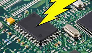
ESD failure mechanisms
There are a number of ways in which ESD can damage semiconductor components. The most obvious results from the very high static voltage, giving rise to high levels of peak current that can cause local burn out. Even though the current flows for a very short period of time the minute feature sizes in the integrated circuit means that damage is caused very easily. The interconnecting wire links or areas in the chip itself can be fused by the high peak current.
Another way in which damage can occur as a result of ESD is when the high level of voltage causes breakdown to occur in a component in the device itself. It may breakdown an oxide layer in the device rendering the device inoperable. With dimensions in some ICs of much less that a micron, it is hardly surprising that even relatively low voltages can cause breakdown.
While damage from ESD can instantly destroy devices, it is also possible for them to create what are termed latent failures. This occurs because ESD does not completely destroy the device, but the damage caused only weakens it, leaving it at risk of failing later in its life. These latent defects cannot usually be detected. The result is that the overall level of reliability is considerably reduced, or (more in the case of analogue devices) the performance may be degraded. Latent failures caused by ESD can be very costly because repair while an item is in service is far more costly than fixing an item that ahs failed in the factory. The reason for this is that a repair technician normally needs to repair the item on site, or it needs to be shipped to a repair facility.
Latent failures may be caused when an interconnection is partially fused by ESD. Often part of the conductor has been destroyed by the static discharge leaving it vulnerable later. Another way in which chips are damaged is when material resulting from damage is spread over the surface of the semiconductor, and this may result in alternative conduction paths.
As a result of the fact that components can be easily damaged by ESD, most manufacturers treat all semiconductors as static sensitive devices, and along with this many handle all devices including passive components like capacitors and resistors as being static sensitive as well. When looking at this it must be remembered that most mass produced pieces of equipment today use surface mount components where the dimensions are much smaller than the traditional components and this makes them far more susceptible to damage from ESD.
More Construction Ideas & Concepts:
Soldering
SMT component soldering
ESD - Electro-Static Discharge
PCB manufacture
PCB assembly
Return to Constructional Techniques menu . . .