JTAG Interface, TAP Test Access Port
Overview of the details of the boundary scan, IEEE1149 or JTAG interface, connector and port.
Boundary Scan JTAG Includes:
What is Boundary Scan / JTAG
Boundary scan description language, BSDL
Design for test with boundary scan
JTAG Spec & IEEE 1149 Standard
JTAG TAP & connector
IEEE 1149.6 (AC coupled JTAG)
Compact JTAG cJTAG IEEE 1149.7
IJTAG, IEEE 1687
In order to be able to use the boundary scan, JTAG system it is necessary to be able to communicate correctly with any board that is set up to use JTAG. The JTAG interface has a number of lines that are used and together these are collectively known as the Test Access Port, TAP. This JTAG port is used for JTAG control as well as providing connections by which the serial data may enter and leave the board.
On some items of electronics equipment there may be a specific JTAG connector or interface into which a JTAG tester may be connected. This approach is particularly useful for any field test that be required as the item under test can be accessed without the need for complete disassembly of the unit.
For most units there is no specific JTAG connector. Instead the connections to the JTAG interface are routed via the main connector to the assembly. These connections would not always be used for the main operation of the unit unless the JTAG test is required as part of the Built in Self Test, BIST where the JTAG controller is located externally to this board or assembly.
JTAG interface signals
There is a maximum of five lines that may be used for a JTAG interface, although one of them is optional and therefore may not always be present. This may be the case when the design becomes short of pins on a connector and the optional one can be sacrificed.
The signals that may be used are given below:
- TCK - Test Clock: The test clock pin on the JTAG interface is the clock signal used for ensuring the timing of the boundary scan system. The Test Clock is used to load the test mode data from the TMS pin, and the test data on the TDI pin on the rising edge. On the falling edge test clock outputs the test data on the TDO pin. It is important that the clock line is properly terminated to prevent reflections that may give rise to false triggering and incorrect operation of the JTAG interface.
- TDI - Test Data Input: The TDI pin on the JTAG interface or JTAG connector is the connection onto which the test instructions data stream is passed. It receives serial input data which is either feed to the test data registers or instruction register, dependent upon on the state of the TAP controller. The TDI line has an internal pull-up, and therefore the input is high with no input.
- TDO - Test Data Output: This pin within the JTAG interface provides data from the boundary scan registers, i.e. test data shifts out on this pin. It delivers serial data which comes from either the test data registers or instruction register, dependent upon on the state of the TAP controller. Data applied to the TDI pin will appear at the TDO pin but may be shifted by a number of clock cycles, depending on the length of the internal register. The TDO pin has a high-impedance.
- TMS - Test Mode Select: This input on the JTAG interface also clocks through on the rising edge of TCK determines the state of the TAP controller. It controls the operation of the test logic, by receiving the incoming data. The value at the input on the rising edge of the clock controls the movement through the states of the TAP controller. The TMS line has an internal pull-up, and therefore the input is high with no input.
- TRST - Test Reset: This is an optional active low test reset pin on the JTAG interface. It permits asynchronous TAP controller initialization without affecting other device or system logic. The TRST signal is usually asynchronous, but not always so dependent upon the particular device in question.
If a TRST connection is not available, then the test logic can be reset by using TCK and TMS in a synchronous fashion. Note that resetting test logic does not imply resetting other circuits: there are generally processor-specific JTAG operations which are able to reset all or part of the device being tested.
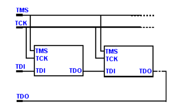
As seen above, the JTAG connections are implemented on the board by daisy chaining devices residing on the JTAG bus i.e. one to the next and so forth in a serial fashion. The TDO pin of one device connects to the TDI pin of the next device. In some instances there may be more than one JTAG connector.
JTAG connector
The JTAG interface is generally an integral part of any electronics assembly. While some items of equipment may provide a specific JTAG port for field test, this is not always the case. In these cases the JTAG interface may accessible via the main assembly connector for which there are a few dedicated pins used for JTAG boundary scan testing. The pins that make up the JTAG interface would not be used under normal operational circumstances.
In addition to the standardised JTAG connections defined above, the JTAG interface may also be expanded to provide additional functionality for debug. Many chip manufacturers have their own proprietary additional connections that work together with the basic JTAG signals to provide a considerable degree of additional functionality.
These additional lines are generally vendor specific, although a new standard known as IJTAG defined under IEEE 1687 provides standardisation to the additional lines and functionality.
Read more about IJTAG IEEE 1687
Connector types
There is no standard for the connector type that should be used for the JTAG connection. Different vendors use different JTAG connector types, often in the form of headers. Different types may also be used between development and production, and in some cases multiple headers may be incorporated to enable different tool support. On some production boards, test points or connections within existing connectors may be used.
There are some common points which are tabulated below:
| Parameter | Details |
|---|---|
| Connection pitch | 0.1 inch (2.54 mm) pin spacing, or occasionally edge connector. |
| Connector mechanicals | Shrouded header recommended to prevent incorrect insertion. |
| Noise immunity | Good practice to ground every other pin. |
When connecting to the JTAG interface, care must be taken to keep leads and internal PCB links as short as possible to preserve the signal integrity and timing.
More Test Topics:
Data network analyzer
Digital Multimeter
Frequency counter
Oscilloscope
Signal generators
Spectrum analyzer
LCR meter
Dip meter, GDO
Logic analyzer
RF power meter
RF signal generator
Logic probe
PAT testing & testers
Time domain reflectometer
Vector network analyzer
PXI
GPIB
Boundary scan / JTAG
Data acquisition
Return to Test menu . . .