Surface Mount Technology & SMT Devices
Surface mount technology, SMT and its associated surface mount devices, SMDs considerably speed up PCB assembly as the components simply mount on the board.
Surface Mount Technology, SMT Includes:
What is SMT
SMD packages
Quad flat pack, QFP
Ball grid array, BGA
Plastic leaded chip carrier, PLCC
Look inside any piece of commercially made electronic equipment these days and it is filled with minute devices. Rather than using traditional components with wire leads like those that may be used for home construction and kits, these components are mounted onto the surface of the boards and many are minute in size.
This technology is known as Surface Mount Technology, SMT and it has the associated SMT components or surface mount devices or SMDs.
Virtually all today's equipment that is manufactured commercially uses surface mount technology, SMT, because it offers significant advantages during PCB manufacture, and in view of the size the use of SMT components enables far more electronics to be packed into a much smaller space.
In addition to the size, surface mount technology allows automated PCB assembly and soldering to be used, and this brings significant improvements in reliability as well as enormous savings in cost.
What actually is surface mount technology?
During the 1970s and 1980s the level of automation started to rise for PCB assembly for boards used in a variety of equipment. The use of traditional components with leads did not prove easy for PCB assembly.
Resistors and capacitors needed to have their leads pre-formed so that they would fit through holes, and even integrated circuits needed to have their leads set to exactly the right pitch so that they could be placed through the holes easily.
This approach always proved difficult as leads often missed the holes as tolerances required to ensure they fitted exactly through the holes were very tight. As a result operator intervention was frequently required to resolve the issues of components not fitting properly and stopping the machines. This slowed down the PCB assembly process and considerably increased costs.
For PCB assembly there is actually no need for the component leads to pass through the board. Instead it is quite adequate for components to be soldered directly to the board. As a result, surface mount technology, SMT was born, and the use of SMT components rose very rapidly as their advantages were seen and realised.

Today surface mount technology is the main technology used for PCB assembly within electronics manufacturing. SMT components are able to be made very small, and may types are used in their billions, particularly SMT capacitors and SMT resistors.
SMT devices
Surface mount components are different to their leaded counterparts. Rather than being designed to wire between two points, SMT components are designed to be set down on a board and soldered to it.
Their leads to not go through holes in the board as might be expected for a traditional leaded component. There are different styles of package for different types of component. Broadly the package styles can be fitted into three categories: passive components, transistors and diodes, and integrated circuits and these three categories of SMT components are viewed below.
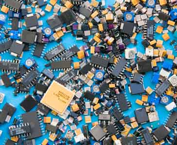
Passive SMDs: There is quite a variety of different packages used for passive SMDs. However the majority of passive SMDs are either SMT resistors or SMT capacitors for which the package sizes are reasonably well standardised. Other components including coils, crystals and others tend to have more individual requirements and hence their own packages.
Resistors and capacitors have a variety of package sizes. These have designations that include: 1812, 1206, 0805, 0603, 0402, and 0201. The figures refer to the dimensions in hundreds of an inch. In other words the 1206 measures 12 x 6 hundredths of an inch.
The larger sizes such as 1812 and 1206 were some of the first that were used. They are not in widespread use now as much smaller components are generally required. However they may find use in applications where larger power levels are needed or where other considerations require the larger size.
The connections to the printed circuit board are made through metallised areas at either end of the package.
Transistors and diodes: SMT transistors and SMT diodes are often contained in a small plastic package. The connections are made via leads which emanate from the package and are bent so that they touch the board. Three leads are always used for these packages. In this way it is easy to identify which way round the device must go.
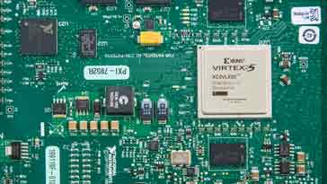
Integrated circuits: There is a variety of packages which are used for integrated circuits. The package used depends upon the level of interconnectivity required. Many chips like the simple logic chips may only require 14 or 16 pins, whereas other like the VLSI processors and associated chips can require up to 200 or more. In view of the wide variation of requirements there is a number of different packages available.
For the smaller chips, packages such as the SOIC (Small Outline Integrated Circuit) may be used. These are effectively the SMT version of the familiar DIL (Dual In Line) packages used for the familiar 74 series logic chips. Additionally there are smaller versions including TSOP (Thin Small Outline Package) and SSOP (Shrink Small Outline Package).
The VLSI chips require a different approach. Typically a package known as a quad flat pack is used. This has a square or rectangular footprint and has pins emanating on all four sides. Pins again are bent out of the package in what is termed a gull-wing formation so that they meet the board. The spacing of the pins is dependent upon the number of pins required. For some chips it may be as close as 20 thousandths of an inch. Great care is required when packaging these chips and handling them as the pins are very easily bent.
Other packages are also available. One known as a BGA (Ball Grid Array) is used in many applications. Instead of having the connections on the side of the package, they are underneath. The connection pads have balls of solder that melt during the soldering process, thereby making a good connection with the board and mechanically attaching it. As the whole of the underside of the package can be used, the pitch of the connections is wider and it is found to be much more reliable.
A smaller version of the BGA, known as the microBGA is also being used for some ICs. As the name suggests it is a smaller version of the BGA.
With the level of adoption for surface mount technology, there is a huge variety of components available. The selection of components available in surface mount packages far exceeds the number available in traditional leaded forms. This is purely because of the demand.
However the popular basic components like transistors and many logic and analogue ICs such as operational amplifiers normally have versions available as a traditional leaded component and also as a surface mount component. A BC109 transistor, for example can be obtained in both formats, as can many operational amplifiers and basic logic chips.
Surface mount technology in design
The main reason for the move to surface mount technology was the great improvement in terms of speed, reliability and cost for the PCB assembly process. Whilst this is the major impact for the adoption of the technology, it also impacts the design and development of new electronic circuits and equipment. Fortunately this transfer brings more advantages to development and circuit performance, than disadvantages.
For the development engineer, the use of surface mount technology offers many advantages, although there are some points to watch:
- Low spurious capacitance and inductance: In view of the small size of the components, the levels of spurious inductance and capacitance are much smaller - SMT resistors function in a way that is closer to the perfect resistor than that of a leaded resistor. Similarly an SMT capacitor will exhibit much lower parasitic inductance. As a result faster speeds and higher frequencies are possible with standard SMT components than would be possible with leaded equivalents.
- Lower power ratings: The power rating of surface mount components is of great importance. The surface mount resistor is the particular example. A standard leaded resistor can dissipate at least 0.25 watts. For surface mount resistors, bing much smaller, the dissipation is also less. Be aware of this and check the manufacturers data.
- Smaller / more dense circuits: As the drive for more functionality within ever smaller volumes is a common trend across the electronics industry, surface mount technology helps in a major way in allowing for miniaturisation. The components can be made much smaller and additionally they can be mounted on the printed circuit board far closer together than would be possible with traditional leaded components. Combined with the greater level of functionality now obtainable within integrated circuits, this means that the task of the development engineer is made possible.
Although there are a few additional precautions to observe when using surface mount technology in a new design, most elements of the design remain very much the same, although the designs tend to be much more complicated and provide much more functionality. In this way the introduction and use of surface mount technology has facilitated the development of electronics, allowing much greater levels of complexity and providing more capability.
PCB assembly using surface mount technology
SMT is used almost exclusively for the PCB assembly and manufacture these days. It is possible to pack far more electronics into a smaller space using SMT. The surface mount components are smaller and often offer a better level of performance and they can be used with automated pick and place machine that in many cases all bit eliminate the need for manual intervention in the assembly process.
Wired components were always difficult to place automatically because the wires needed to be pre-formed to fit the relevant hole spacing, and even then they were prone to problems with placement.
Today in the PCB assembly process, most of the components on a board are placed automatically. Occasionally some may need manual intervention, but this is being reduced all the time. Traditionally some connectors and possibly a few other components required assisted placement, but the level of manual placement is falling all the time.
Today, printed circuit boards are normally developed to reduce this to an absolute minimum, even to the extent of altering the design to use components that can be placed automatically. In addition to this, component manufacturers have developed some specialised surface mount versions of components that enable virtually complete automated assembly for most boards.
One of the issues with some components has been their resilience to heat. The soldering processes require that the whole component is raised to a high temperature, and this has caused issues with some technologies. Integrated circuits, surface mount resistors and many types of surface mount capacitor are fine.
However, it was for this reason that surface mount electrolytic capacitors were not used initially. Instead surface mount tantalums were used, but now, versions of surface mount electrolytic capacitors have been developed that are able to tolerate the temperatures experienced during soldering.
There are other components that have required special development to enable them to become available in surface mount component formats.
Board expansion & flexure
One of the issues that can occur with surface mount boards arise as a result of temperature changes and also board flexing. With boards using leaded components this is not a major issue because the wires on the components take up the movement and relieve any strain that may be caused.
The same may not be true for surface mount components. The components are soldered down tot he printed circuit board and quite rigidly held in place. Components like surface mount transistors and surface mount integrated circuits where there are leads from the device body onto the surface of the board have some means for accommodating movement, but surface mount resistors and capacitors do not.
The components most sensitive to strain on the board are surface mount capacitors - the ceramic MLCC variety. They tend to crack when put under tensile stress. This obviously is a major issue for reliability.
There are several precautions that can be taken in design and PCB assembly to ensure that warping and temperature expansion etc problems are minimise:
- Ensure PCB power and earth planes are distributed evenly: When the printed circuit boards are passed though the soldering process during PCB assembly, the boards will be heated significantly and this can lead to warping - the levels can be significant in some large boards. To help alleviate this issue, earth planes and power planes should cover the complete board as far as possible. If they are only present over part of the printed circuit board this can cause warping.
- Shape of components: Surface mount components with short, wide bodies are preferable to long and thin ones. If the component is short and wide, the effects of expansion and flexing will be less pronounced.
- Mount components at right angle to direction of maximum flex: Boards tend to warp along the longest length of the board. Mount components in a plane that will be exposed to the minimum flex or bend.
SMT applications
Although it is possible to use some SMT components for home construction, great care is required when soldering them. Additionally even the ICs having a wide pin spacing may be difficult to solder.
Those with fifty or more pins cannot be soldered without special equipment. They are intended only for large scale manufacturing. Even when working on boards that have already been built great care is needed. However these SMT components offer great cost savings to manufacturers and this is why they have been adopted. Fortunately for the home constructor, traditional leaded components that can be soldered manually are still widely available and offer a much better solution for home construction.
Nevertheless SMT components can be used for some home projects where they are applicable - where the SMT component leads and connections are not too small to manage with more traditional soldering irons and other tools.
More Electronic Components:
Batteries
Capacitors
Connectors
Diodes
FET
Inductors
Memory types
Phototransistor
Quartz crystals
Relays
Resistors
RF connectors
Switches
Surface mount technology
Thyristor
Transformers
Transistor
Unijunction
Valves / Tubes
Return to Components menu . . .