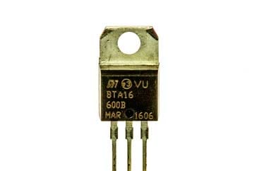
What is a Triac?
Triacs are semiconductor devices that are widely used for switching medium power AC - their advantage is that they can switch both halves of alternating cycle.
Triac, Diac, SCR Tutorial Includes:
Thyristor basics
Thyristor device structure
Thyristor operation
Gate turn off thyristor, GTO
Thyristor specifications
What is a triac
Triac specifications
Diac overview
Triacs are electronic components that are widely used in AC power control applications. They are able to switch high voltages and high levels of current, and over both parts of an AC waveform. This makes triac circuits ideal for use in a variety of applications where power switching is needed.
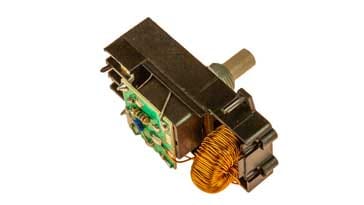
One particular use of triac circuits is in light dimmers for domestic lighting, and they are also used in many other power control situations including motor control and electronic switches.
As a result of their performance, triacs tend to be used for low to medium power electronic switching applications, leaving thyristors to be used for the very heat duty AC power switching applications.
Triac basics
The triac is a development of the thyristor. While the thyristor can only control current over one half of the cycle, the triac controls it over two halves of an AC waveform.

As such the triac can be considered as a pair of parallel but opposite thyristors with the two gates connected together and the anode of one device connected to the cathode of the other, etc..
The fact that the triac switching action occurs on both halves of an AC waveform means that for AC electronic switching applications, the complete cycle can be used.
For basic thyristor circuits, only half the waveform is used and this means that basic circuits using thyristors will not utilise both halves of the cycle. Two devices are required to utilise both halves.
However the triac only requires one device to control both halves of the AC waveform and in many respects it is an ideal solution for an electronic switch for AC.
Triac symbol
Like other electronic components, the triac has its own circuit symbol for use on circuit diagrams and this indicates its bi-directional properties. The triac symbol can be seen to be a couple of thyristor symbols in opposite senses merged together.

Like a thyristor, a triac has three terminals. However the names of these are a little more difficult to assign, because the main current carrying terminals are connected to what is effectively a cathode of one thyristor, and the anode of another within the overall device.
There is a gate which acts as a trigger to turn the device on. In addition to this the other terminals are both called Anodes, or Main Terminals These are usually designated Anode 1 and Anode 2 or Main Terminal 1 and Main Terminal 2 (MT1 and MT2). When using triacs it is both MT1 and MT2 have very similar properties.
How does a triac work?
Before looking at how a triac works, it helps to have an understanding of how a thyristor works. In this way the basic concepts can be grasped for the simpler semiconductor device and then applied to a triac which is more complicated.
For the operation of the triac, it can be imagined from the circuit symbol that the triac consists of two thyristors in parallel but around different ways. The operation of the triac can be looked on in this fashion, although the actual operation at the semiconductor level is rather more complicated.

The triac structure is shown below and it can be seen that there are several areas of N-type and P-type material that form what is effectively a pair of back to back thyristors.

The triac is able to conduct in a number of ways - more than the thyristor. It can conduct current irrespective of the voltage polarity of terminals MT1 and MT2. It can also be triggered by either positive or negative gate currents, irrespective of the polarity of the MT2 current. This means that there are four triggering modes or quadrants:
- I+ Mode MT2 current is +ve, gate current is +ve
- I- Mode MT2 current is +ve, gate current is -ve
- III+ Mode: MT2 current is -ve, gate current is +ve
- III- Mode: MT2 current is -ve, gate current is -ve
It is found that the triac trigger current sensitivity is greatest when the MT2 and gate currents are both of the same polarity, i.e. both positive or both negative. If the gate and MT2 currents are of the opposite polarity then the sensitivity is typically about half the value of when they are the same.
The typical IV characteristic of a triac can be seen in the diagram below with the four different quadrants labelled.

Triac applications
Triacs are used in many applications. These electronic components are often used in low to medium power AC switching requirements. Where large levels of power need to be switched, two thyristors / SCRs tend to be used as they can be controlled more easily.
Nevertheless triacs are widely used in many applications:
- Lighting control - especially domestic dimmmers.
- Control of fans and small motors.
- Electronic switches for general AC switching and control
There are naturally many other triac applications, but these are some of the most common.
In one specific application, triacs can be included in modules called solid state relays. Here an optical version of this semiconductor device is activated by an LED light source turning the solid state relay on according to the input signal.
Typically within solid state relays, the LED light or infrared source and the optical triac are contained within the same package, sufficient isolation being provided to withstand high voltages which may extend to hundreds of volts or possibly even more.
Solid state relays come in many forms, but those used for AC switching may use a triac.
Using triacs
There are a number of points to note when using triacs. Although these semiconductor devices operate very well, to get the best performance out of them it is necessary to understand a few hints on tips on using triacs.
It is found that because of their internal construction and the slight differences between the two halves, these electronic components do not fire symmetrically. This results in harmonics being generated: the less symmetrical the triac fires, the greater the level of harmonics that are produced.
It is not normally desirable to have high levels of harmonics in a power system and as a result triacs are not favoured for high power systems. Instead for these systems two thyristors may be used as it is easier to control their firing.
To help in overcoming the problem of the triac non-symmetrical firing, and the resulting harmonics, another semiconductor device known as a diac (diode AC switch) is often placed in series with the gate of the triac.
The inclusion of this semiconductor device helps make the switching more even for both halves of the cycle and thereby creating a more effective electronic switch.
This results from the fact that the diac switching characteristic is far more even than that of the triac. Since the diac prevents any gate current flowing until the trigger voltage has reached a certain voltage in either direction, this makes the firing point of the triac more even in both directions.
Triac circuit examples
There are many ways in which triacs can be used. The two examples below give a taste of what can be done with these semiconductor devices.
- Simple triac electronic switch circuit: The triac can function as an electronic switch - it could enable a trigger pulse of a low power switch to turn the triac on to control a much higher power levels that might be possible with a simple switch.

Simple triac switch circuit - Triac variable power or dimmer circuit: One of the most popular triac circuits varies the phase on the input of the triac to control the power that can be dissipated into load.

A basic triac circuit using phase of input waveform to control dissipated power in the load
There are many more triac circuits that can be used. The device is very versatile and can be used in a variety of circuits, typically to provide various forms of AC switching.
Note on Triac Circuits & Design:
Triac circuits are able to switch both halves on an alternating waveform using single device and this makes them very attractive for use in many small to medium power AC switching circuits.
Read more about Triac Circuits & Design
Triac specifications
Triacs have many specifications that are very similar to those of thyristors, although obviously they are intended for triac operation on both halves of a cycle and need to be interpreted as such.
However as their operation is very similar, so too are the basic specification types. Parameters like the gate triggering current, repetitive peak off-state voltage and the like are all required when designing a triac circuit, ensuring there is sufficient margin for the circuit to operate reliably.
Triacs are ideal devices for use in many AC small power applications. Triac circuits for use as dimmers and small electronic switches are widespread and they are simple and easy to implement. When using triacs, diacs are often included in the circuit as mentioned above to help reduce the level of harmonics produced.
More Electronic Components:
Batteries
Capacitors
Connectors
Diodes
FET
Inductors
Memory types
Phototransistor
Quartz crystals
Relays
Resistors
RF connectors
Switches
Surface mount technology
Thyristor
Transformers
Transistor
Unijunction
Valves / Tubes
Return to Components menu . . .