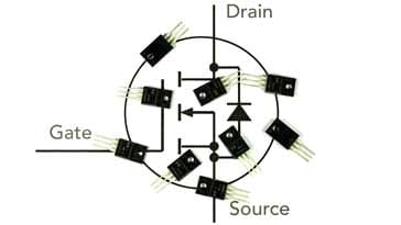
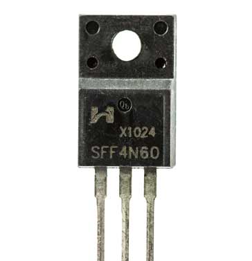
Power MOSFET
Power MOSFTs are used in many power supply and general power applications, especially as switches. Variant s include planar MOSFETs, VMOS, UMOS TrenchMOS, HEXFETs and other different brand names.
FETs, Field Effect Transistors Includes:
FET basics
FET specifications
JFET
MOSFET
Dual gate MOSFET
Power MOSFET
MESFET / GaAs FET
HEMT & PHEMT
FinFET technology
IGBT
Silicon carbide, SiC MOSFET
GaN FET / HEMT
MOSFET technology is ideal for use in many power applications, where the low switch on resistance enables high levels of efficiency to be attained.
There is a number of different varieties of power MOSFET available from different manufacturers, each with its own characteristics and abilities.
Many power MOSFETs incorporate a vertical structure topology. This enables high current switching with high efficiency within a relatively small die area. It also enables the device to support high current and voltage switching.
Power MOSFET types
Within the overall arena of power MOSFETs, there are a number of specific technologies that have been developed and addressed by different manufacturers. They use a number of different techniques that enable the power MOSFETs to carry the current and handle the power levels more efficiently. As already mentioned they often incorporate a form of vertical structure
The different types of power MOSFET have different attributes and therefore can be particularly suited for given applications.
- Planar power MOSFET: This is the basic form of power MOSFET. It is good for high voltage ratings because the ON resistance is dominated by the epi-layer resistance. This structure is generally used when a high cell density is not needed.
- VMOS: VMOS power MOSFETs have been available for many years. The basic concept uses a V groove structure to enable a more vertical flow of the current, thereby providing lower ON resistance levels and better switching characteristics. Although used for power switching, they may also be used for high frequency small RF power amplifiers.
- UMOS: The UMOS version of the power MOSFET uses a grove similar to that the VMOS FET. However the grove has a flatter bottom to it and provides some different advantages.
- HEXFET: This form of power MOSFET uses a hexagonal structure to provide the current capability.
- TrenchMOS: Again the TrenchMOS power MOSFET uses a similar basic grove or trench in the basic silicon to provide better handling capacity and characteristics. In particular, Trench power MOSFETs are mainly used for voltages above 200 volts because of their channel density and hence their lower ON resistance.
Power MOSFET breakdown voltage
The breakdown voltage is a key parameter for any power device including power MOSFETs. As these devices may operate a voltages well in excess of those encountered in lower power electronic circuits, the voltage breakdown voltage is an important aspect of any power MOSFET device.
In most power MOSFETs the N+ source termination and the P body junction are shorted using source metallisation. This avoids the possibility of spurious turn on of the parasitic bipolar transistor within the structure.
In operation, when no bias is applied to the gate, then the device is able to provide a high drain voltage through the reverse biased P type body and N+ epitaxial layer junction (shown as P-silicon and N- on the planar power MOSFET diagram). When high voltages are present, most of the applied voltage appears across the lightly doped N- layer. If a higher operational voltage is required, then the N- layer can be more lightly doped and made thicker, but this also has the effect of increasing the ON resistance.
For lower voltage devices, the doping levels for the P silicon areas and the N- become comparable and the voltage is shared across these two layers. However if the P silicon area is not thick enough then it can be found that the depletion region can punch through to the N+ source region, giving rise to a lower breakdown voltage.
On the other hand, if the device is designed for too high a voltage, then the channel resistance and threshold voltage will increase. As a result careful optimisation of the device is needed. Also when choosing power MOSFET devices, it is necessary to opt for one that provides the correct combination of breakdown voltage and ON resistance.
Capacitance
The switching behaviour of any power MOSFET is greatly affected by the levels of parasitic capacitance that occurs within the device.
The main areas of capacitance that affect the switching performance are gate to source capacitance CGS; gate to drain capacitance, CGD; and the drain to source, CDS.
These capacitances are non-linear and they are dependent upon the device structure and the voltages present at any given time. Thy result from the bias dependent oxide capacitance and the bias dependent depletion layer capacitance. Typically as the voltages increase, so the depletion layers increase and the capacitance levels decrease.
Power MOSFET threshold voltage
The threshold voltage which is normally designated as VGS(TH) is the minimum gate voltage that can form a conducting channel between the source and the drain.
For power MOSFETs the this threshold voltage is normally measured for a drain source current of 250µA.
The threshold voltage is determined by factors in the power MOSFET including the gate oxide thickness and the doping concentration in the channel.
Power MOSFET applications
Power MOSEFET technology is applicable to many types of circuit. Applications include:
- Linear power supplies
- Switching power supplies
- DC-DC converters
- Low voltage motor control
Power MOSFETs are normally used in applications where voltages do not exceed about 200 volts. Higher voltages are not so easily achievable. Where the Power MOSFETs are used, it is their low ON resistance that is particularly attractive. This reduces power dissipation which reduces cost and size less metalwork and cooling is required. Also the low ON resistance means that efficiency levels can be maintained at a higher level.
More Electronic Components:
Batteries
Capacitors
Connectors
Diodes
FET
Inductors
Memory types
Phototransistor
Quartz crystals
Relays
Resistors
RF connectors
Switches
Surface mount technology
Thyristor
Transformers
Transistor
Unijunction
Valves / Tubes
Return to Components menu . . .