JFET - Junction Field Effect Transistor
The junction field effect transistor, JFET is an active electronic component which is one of the workhorses of the electronics industry providing a good balance between cost and performance.
FETs, Field Effect Transistors Includes:
FET basics
FET specifications
JFET
MOSFET
Dual gate MOSFET
Power MOSFET
MESFET / GaAs FET
HEMT & PHEMT
FinFET technology
IGBT
Silicon carbide, SiC MOSFET
GaN FET / HEMT
The junction field effect transistor or JFET is widely used in electronic circuits. The junction field effect transistor is a reliable and useful electronic component that can be used very easily in a variety of electronic circuits ranging from amplifiers to switch circuits.
The junction field effect transistor is widely available, and these semiconductor devices can be bought for very little money. This makes them ideal for use in many electronic circuits where a good balance between cost and performance is of interest.
JFETs have been available for many years, and although they don't offer the exceedingly high levels of DC input resistance of the MOSFET, they are nevertheless very reliable, robust and easy to use. This makes these electronic components an ideal choice for many electronic circuit designs. Also the components are available in both leaded and surface mount device formats.
JFET basics
Basically a field effect transistor or FET consists of a section of silicon whose conductance is controlled by an electric field. The section of silicon through which the current flows is called the channel, and it consists of one type of silicon, either N-type or P-type.

The connections at either end of the device are known as the source and drain. The electric field to control the current is applied to a third electrode known as a gate.
As it is only the electric field that controls the current flowing in the channel, the device is said to be voltage operated and it has a high input impedance, usually many megohms. This can be a distinct advantage over the bipolar transistor that is current operated and has a much lower input impedance.
JFET operation
The Junction FET is a voltage controlled device. In other words, voltages appearing on the gate, control the operation of the device.
Both N-channel and P-channel devices operate in similar ways, although the charge carriers are inverted, i.e. electrons in one and holes in the other. The case for the N-channel device will be described as this is the more commonly type used.

The thickness of this layer varies in accordance with the magnitude of the reverse bias on the junction. In other words when there is a small reverse bias the depletion layer only extends a small way into the channel and there is a large area to conduct current.
When a large negative bias is placed on the gate, the depletion layer increases, extending further into the channel, reducing the area over which current can be conducted.
With increasing bias the depletion layer will eventually increase to the degree that it extends right across the channel, and the channel is said to be cut off.
When a current flows in the channel the situation becomes slightly different. With no gate voltage electrons in the channel (assuming an n-type channel) will be attracted by the positive potential on the drain, and will flow towards it enabling a current to flow within the device, and hence within the external circuit.
The magnitude of the current is dependent upon a number of factors and included the cross sectional area of the channel, its length and conductivity (i.e. the number of free electrons in the material) and the voltage applied.
From this it can be seen that the channel acts as a resistor, and there will be a voltage drop along its length. As a result of this it means that the p-n junction becomes progressively more reverse biased as the drain is approached. Consequently the depletion layer takes becomes thicker nearer the drain as shown.
As the reverse bias on the gate is increased a point is reached where the channel is almost closed off by the depletion layer. However the channel never completely closes. The reason for this is that the electrostatic forces between the electrons cause them to spread out, giving a counter effect to the increase in thickness of the depletion layer.
After a certain point the field around the electrons flowing in the channel successfully opposes any further increase in the depletion layer. The voltage at which the depletion layer reaches its maximum is called the pinch off voltage.
JFET circuit applications
JFETs are very useful electronic components and as a result they are used in many electronic circuit designs. They offer a number of distinct advantages that can be put to use in many circuits.
- Simple biasing
- High input impedance
- Low noise
In view of their characteristics, JFETs are seen in many circuits ranging from amplifiers to oscillators, and logic switches to filters and many more applications.
Note on Field Effect Transistor Circuit Design:
The field transistor transistors can be used in many types of circuits although the three basic configurations are common source, common drain (source follower) and common gate. The circuit design itself if fairly straightforward and can be undertaken quite easily.
Read more about Field Effect Transistor Circuit Design
JFET structure & fabrication
JFETs can be either N-channel of P-channel devices. They can be made in very similar manners, the main exception being that the N and P areas in the structure below are interchanged.
Often devices are made within a larger substrate and the FET itself fabricated as shown in the diagram below.

There are a number of ways in which FETs can be fabricated. For silicon devices a heavily doped substrate normally acts as a second gate.
The active n-type region may then be grown using epitaxy, or it may be formed by diffusing the impurities into the substrate or by ion implantation.
Where gallium arsenide is used the substrate is formed from a semi-insulating intrinsic layer. This reduces the levels of any stray capacitances and enables good high frequency performance to be obtained.
Whatever the material used for the FET, the distance between the drain and source is important and should be kept to a minimum. This reduces the transit times where high frequency performance is required, and gives a low on resistance that is vital when the device is to be used for power or switching applications.
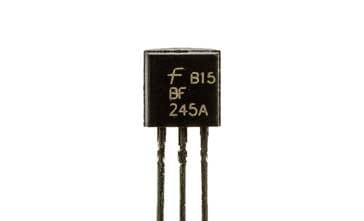
In view of their popularity, JFETs are available in a variety of packages. They are widely available as leaded electronic components on the popular TO92 plastic package as well as a number of others. Then as surface mount devices they are available in packages including SOT-23 and SOT-223. It is probably as surface mount devices that JFETs are most widely used. Most large scale production is undertaken using surface mount technology and the accompanying surface mount devices.
JFET characteristics
There are several different characteristics that are used to define the performance of a JFET. The output or drain characteristics along with the transfer characteristics are key to the operation of these electronic components. These are key to the electronic circuit design and understanding them is important when using them.
The various types of JFET characteristics will be addressed in turn.<.p>
JFET Drain Characteristic With Shorted-Gate: there are two ways in which the output characteristic of a junction field effect transistor can be specified. One is with the gate shorted to zero volts. This gives a single curve for the semiconductor device and shows how it operates under these conditions.
JFET Drain Characteristics With External Bias: It is also important to understand how the junction FET operates under conditions if different levels of bias. When this is done, curves fort he characteristics under different bias levels are given.
JFET Transfer Characteristic: The transfer characteristic for a junction field effect transistor show the effect of the variations of gate voltage, VGSM affect the output or drain current, ID.
Although the JFET is less popular than the MOSFET and fewer JFETs, it is still a very useful semiconductor device. Offering high input impedance, simple biasing, low noise, and a low cost, it provides a high level of performance which can be used in many situations.
More Electronic Components:
Batteries
Capacitors
Connectors
Diodes
FET
Inductors
Memory types
Phototransistor
Quartz crystals
Relays
Resistors
RF connectors
Switches
Surface mount technology
Thyristor
Transformers
Transistor
Unijunction
Valves / Tubes
Return to Components menu . . .