Transistor Emitter Follower Circuit: Common Collector Amplifier
The emitter follower or common collector circuit provides an ideal buffer amplifier and it is easy to design the circuit.
Transistor Circuit Design Tutorial Includes:
Transistor circuit design
Circuit configurations
Common emitter
Common emitter circuit design
Emitter follower
Common base
See also:
Transistor circuit types
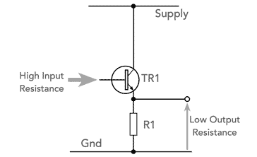
The common collector circuit configuration is more widely known as the emitter follower and it provides a high input impedance and a low output impedance.
This means that the emitter follower circuit provides an ideal buffer stage, and as a result it is used in many circuits where there is a need not to load a circuit like an oscillator or other circuit, but provide a lower impedance to the following stages.
The electronic circuit design for the emitter follower or common collector stage is very straightforward requiring just a few electronic components and some very simple calculations.
Emitter follower / common collector transistor amplifier basics
The common collector transistor circuit configuration gains its name from the fact that the collector circuit is common to both input and output circuits, the base being associated with only the input, then the emitter with the output only.
The other name for the common collector is emitter follower. This name is derived from the fact that the emitter voltage "follows" that of the base circuit - the circuit has unit voltage gain.
The emitter follower transistor amplifier has a very straightforward circuit. The base is connected to the previous stage, and often this may be directly connected as this can save on additional bias resistors which lower the input impedance and hence increase the loading to the previous stage.

Looking at the circuit it can be seen that although the emitter voltage follows that of the base, in DC terms it is actually less than that of the base by a voltage equal to the PN junction drop between the base and emitter. Typically this is 0.6 volts for a silicon transistor and 0.2 to 0.3 for germanium transistors, although these are not widely used these days.
As the emitter voltage follows that of the base, this means that the input and output are exactly in phase and not shifted by 180° as in the case of the common emitter amplifier.
Emitter follower transistor amplifier characteristics summary
The table below gives a summary of the major characteristics of the common collector, emitter follower transistor amplifier.
| Common collector, emitter follower transistor amplifier characteristics |
|||
|---|---|---|---|
| Parameter | Characteristics | ||
| Current gain | High | ||
| Voltage gain | Zero | ||
| Power gain | Medium | ||
| Input / output phase relationship | 0° | ||
| Input resistance | High | ||
| Output resistance | Low | ||
One key aspect of the characteristic is the input impedance. As it is normally used as a buffer amplifier, this is the key parameter.
The input resistance can easily be calculated for a circuit because it is β times the resistor R1, where β is the forward current gain of the transistor.

DC coupled emitter follower, common collector circuit
The simplest way of connecting an emitter follower is to directly couple the input as shown below. Often the collector of the previous stage will be at approximately the mid rail voltage, and this means that it can be directly coupled to the buffer stage.

- Choose transistor: As with other forms of transistor circuit, the transistor should be chosen to meet the anticipated requirements.
- Emitter resistor value: The voltage on the emitter is easy to define. It is simply that appearing at the previous stage. Say for example this is half the rail voltage, then the voltage on the emitter Q1 will be 0.5V (for a silicon transistor) less than this - the drop of the base emitter junction. Simply calculate the value of the resistor for the current required.
- Emitter follower input resistance: The input resistance of the circuit is effectively β times the emitter resistor, R1.
AC coupled emitter follower, common collector circuit
It is not always possible to directly couple the emitter follower, common collector buffer. When this is the case, it is necessary to add a few additional electronic components: coupling capacitors and bias resistors to the circuit.

The emitter follower can be designed and electronic component values determined using the design flow below as a basis:
- Choose transistor: As before, the transistor type should be chosen according to the anticipated performance requirements.
- Select emitter resistor: Choosing an emitter voltage of about half the supply voltage to give the most even range before the onset of any clipping, determine the current required from the impedance of the following stage.
- Determine base current: The maximum base current is the collector current divided by β (or hfe which is essentially the same).
- Determine the base voltage: The base voltage is simply the emitter voltage plus the base emitter junction voltage - this is 0.6 volts for silicon and 0.2 volts for germanium transistors.
- Determine base resistor values: Assume a current flowing through the chain R1 + R2 of around ten times that of the base current required. Then select the correct ratio of the resistors to provide the voltage required at the base.
- Determine value of input capacitor value: The value of the input capacitor should equal the resistance of the input circuit at the lowest frequency to give a -3dB fall at this frequency. The total impedance of the circuit will be β times R3 plus any resistance external to the circuit, i.e. the source impedance. The external resistance is often ignored as this is likely to not to affect the circuit unduly.
- Determine output capacitor value : Again, the output capacitor is generally chosen to equal the circuit resistance at the lowest frequency of operation. The circuit resistance is the emitter follower output resistance plus the resistance of the load, i.e. the circuit following.
- Re-evaluate assumptions: In the light of the way the circuit has developed, re-assess any circuit assumptions to ensure they still hold valid. Aspects such as the transistor choice, current consumption values, etc.
The emitter follower circuit is particularly useful for applications where a input high impedance is required. Offering a high input impedance and low output impedance it is does not load circuits that may only have a small output capability, or those circuits like oscillators that need a high impedance load to ensure the optimum stability, etc.
Emitter follower practical aspects
When using the emitter follower circuit, there are a useful few practical points to note:
- Input capacitance affects RF: Although the emitter follower offers a high resistance to any signals, the base emitter capacitance may reduce the impedance if signals above a few hundred kilohertz are used. This should be remembered during the electronic circuit design as this can affect any loading levels significantly.
Collector may need decoupling: On some occasions an emitter follower circuit can oscillate, especially if long leads are present. This can happen when high frequency responses are needed and high frequency transistors are used.
One of the easiest ways of preventing this is to decouple the collector to ground using a capacitor, C3 with connections that are as short as reasonably possible. This can be easily incorporated during the electronic circuit design, and can be included as a precautionary measure using just a couple of electronic components.
Values will depend upon the frequency in use. If necessary a small value of resistance, R4, can be placed between the collector and the supply rail. The value of this resistor only needs to be of the order of 100Ω or less in most instances. This can also be added as a precaution.

Emitter follower circuit with collector decoupling The same effect can also be implemented by placing a small ferrite bead over the collector lead. However for most purposes the resistor / capacitor solution is the most convenient.
The emitter follower is simple to implement and requires only a few electronic components. It is a very convenient circuit to add when a circuit requires a minimum load to be placed upon it.
The emitter follower is widely used as a buffer amplifier to reduce the loading on the previous stage and provide a lower impedance output for any following circuits. The electronic circuit design for the stage is also very straightforward and easy to accomplish.
More Circuits & Circuit Design:
Op Amp basics
Op Amp circuits
Power supply circuits
Transistor design
Transistor Darlington
Transistor circuits
FET circuits
Circuit symbols
Return to Circuit Design menu . . .