Thyristor, SCR Circuit Design: circuit design, triggering, etc
Understand the operation, triggering mechanisms and overall circuit design for thyristor or SCR circuits for use in many power applications.
Thyristor Circuit Design Includes:
Thyristor circuit design primer
Overvoltage crowbar
Triac circuits
The thyristor or silicon controlled rectifier, SCR is a particularly useful component and it finds many uses in areas like power control where these components can be used to switch high voltages and currents.
Thyristors have taken over most of the power switching applications that were once handled by relays, although very high voltage contactors are still used.
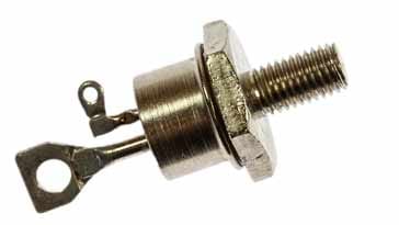
Thyristor or silicon controlled rectifier, SCR design can be undertaken in a straightforward manner. The devices, although a little unusual follow the same basic circuit design rules that govern other components as well.
The main issue is to make sure that all components are adequately rated, as often thyristor circuits are used in high power applications.
Thyristor, SCR circuit basics
The thyristor or silicon controlled rectifier operates in a different way to that of a standard bipolar transistor or FET.
The thyristor has two electrodes that are connected to the main circuit to be controlled. These two electrodes are called the anode and cathode.
A third electrode called the gate is used to control the thyristor within the circuit.

Note on Thyristor Technology:
Thyristors or SCRs are based around a unique structure of a PNPN structure and have three electrodes: anode, cathode and the gate. When the gate receives a triggering current, it fires the thyristor enabling current to flow until the voltage between anode and cathode is removed. This enables the thyristor to switch high voltages and currents, although it only over one half of the cycle. Two can be used to cover both halves of the cycle.
Read more about Thyristor Technology
To understand how the SCR operates within a circuit, it is best to look at its equivalent circuit. From this it can be seen that the SCR can be considered to consist of two interconnected transistors.
Under initial conditions there is no conduction between the anode and cathode. However, if current is applied to the gate in a sense that makes TR2 conduct, the SCR will turn on, but in one direction only. This conduction will be maintained even if the gate current is removed. In this way the gate current can be considered as a trigger impulse.
In order to stop conduction, the voltage between anode and cathode needs to be reduced to below the drop out level. This occurs when one or both of the transistors reach their cut-off mode. At this point conduction of the whole device will stop and the gate will need to be re-triggered.

As can be gathered, the thyristor, SCR only conducts in one direction. When used with an AC signal it needs to be re-triggered for each conduction half cycle.
Once the thyristor, SCR is in its fully conducting state, the voltage drop across the device is generally around 1 V for all values of anode current up to its rated value.
The SCR then continues to conduct while the anode current remain above the holding current for the device which is normally denoted as IH. Below this value the SCR stops conducting. Therefore in DC and some highly inductive AC circuits there has to be a means of turning the device off as the SCR will continue conducting.
Thyristor gate circuit design
In order to prevent overloading the gate and also false triggering, some resistors are often placed in the gate circuit.

When designing an SCR circuit, two gate resistors are often included.
In the diagram R1 is included to limit the gate current to an acceptable level. This resistor is chosen to provide sufficient current to trigger the SCR while not providing so much that the gate junction is placed under stress.
The second resistor, R2 is the gate cathode resistor, sometimes denoted as RGK included to prevent spurious triggering. It effectively reduces the sensitivity of the gate.
Sometimes this resistor may be included within the SCR package itself and no external resistor may be required. It is necessary to check the manufacturers datasheet to determine what is needed.
When designing a thyristor, SCR circuit, special attention needs to be paid to the trigger circuit within any electronic circuit design using these electronic components.
The operation of the whole area of the thyristor or silicon controlled rectifier circuit is largely dependent upon the way in which it triggers.
Ensuring that there are no false triggers whilst also ensuring the thyristor triggers when it is required needs to receive particular attention when the circuit design is undertaken.
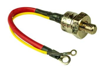
Within the triggering of thyristors or SCRs, various aspects including the gate drive requirements if gate triggering is used, trigger time where the time of the trigger stimulus applied needs to be maintained for the circuit to latch and others are all important.
The importance of the various parameters is, of course, dependent upon the form of SCR triggering used. As a variety of trigger mechanisms are available, it is necessary to be aware of them all to ensure that the correct triggering takes place.
SCR triggering / firing summary
Understanding the different ways in which a thyristor can trigger is a considerable help when undertaking an electronic circuit design using these components.
Knowing the different ways in which the thyristor can trigger can ensure that the device only triggers when it is required, and not when another stimulus actuates the trigger mechanism within the device.
There are several ways in which a thyristor or SCR can be triggered or fired, and not all of them may be obvious at first sight.
• Gate triggering:
This form of SCR triggering is the one that is most commonly seen in electronic circuit designs. It is simple, reliable, efficient and also easy to implement for most applications - a simple trigger signal can be applied, with suitable processing if required.
This means that other electronic circuits can be used to derive a suitable trigger signal and this can then be applied to the SCR gate within the circuit design.
For gate SCR triggering to be used, the SCR must operate below its breakdown voltage, and a suitable safety margin also allowed to accommodate any transients that may occur. Otherwise forward voltage or breakdown triggering may occur.
To turn-on of an SCR, a positive gate voltage between gate and cathode. This gives rise to a gate current where charges are injected into the inner p layer of the device. This effectively reduces the voltage at which forward break-over occurs. It can be gathered that the gate current determines the forward voltage at which the device switches to its conducting state. Higher the gate current, the lower the forward break-over voltage.
There are many simple methods of applying the trigger signal. Possibly one of the simplest arrangements is shown in the diagram below.

Here is can be seen that there are two resistors. The first is R1 which is included to limit the gate current to an acceptable level. This resistor is chosen to provide sufficient current to trigger the SCR while maintaining it within safe limits for the device. It can easily be calculated using the device ratings and Ohms law.
The second resistor, R2 is the gate cathode resistor. This is sometimes denoted as RGK and it is included to prevent spurious triggering. The action of the resistor can be seen with respect to the two transistor analogy of the SCR. It shows that a low external resistance between the gate and cathode bypasses some current around the gate junction.
Accordingly a higher anode current is required to initiate and maintain conduction. It is particularly found that low current high sensitivity SCRs are triggered at very low current levels and therefore an external gate-cathode resistance is required to prevent triggering by thermally generated leakage current in the gate region.
However the gate cathode resistance bypasses some of the internal anode current caused by the rapid rate of change of the anode voltage (dv/dt). It also raises the forward break-over voltage by reducing the efficiency of the NPN transistor region thus requiring a somewhat higher avalanche multiplication effect to initiate the triggering.
The current that bypasses the gate junction also affects the latching and holding currents.
It can therefore be seen that the effects of using the gate cathode bypass resistor include:
- Increase the dv/dt capability.
- Retain gate damping to assure the maximum repetitive peak off-state voltage VDRM capability.
- Raise latching and holding current levels
- Lower the turn-off time, tq.
Although the simple circuit shown above is adequate for many applications, where a more controlled triggering mechanism is required, account needs to be taken of the gate characteristics before triggering, during triggering and afterwards. This is required because the gate characteristics change as a result of the current changes within the device.
• Anode cathode forward voltage SCR triggering:
This form of SCR triggering or firing occurs when the voltage between the anode and cathode causes avalanche conduction to take place. The way in which this occurs can be seen in conjunction with the SCR structure.

When the anode to cathode forward voltage is increased, diode junction, J2, comes under increasing stress as it is reverse biased. Ultimately the voltage gradient will increase beyond the breakdown point and avalanche breakdown will occur triggering the SCR. The voltage at which this occurs is known as the forward break-over voltage VB0.
As the junction J2 breaks down, current will flow and triggering the SCR to its conducting state. The junctions J1, J3 are already forward biased, and therefore the breakdown of junction J2 allows the flow of carriers across all three junctions enabling the load current to flow. As with other forms of triggering the SCR, the device remains in its conducting condition.
The use of this method of turning the device on is not advised because exceeding the value of VB0 could destroy the device. Any circuit should be designed to avoid this method of triggering, noting the maximum of any likely voltage spikes.
• dv/dt triggering:
SCR triggering can also occur without any gate current if the rate of rise of anode to cathode voltage exceeds certain limits for the particular device.
It is important to understand the dV/dt triggering because transient voltages across the thyristor can cause it to trigger, sometimes unexpectedly. It can often be a cause of unwanted and intermittent triggering.
• Temperature triggering:
This form of SCR triggering may occur under some circumstances. It may give rise to unexpected responses and therefore its effects should be noted as part of any design process.
Temperature triggering of SCRs or thyristors occurs as the voltage across the junction J2 and any leakage current may raise the temperature of the junction. The increase in temperature further increases the temperature which will in turn increase the leakage current. This cumulative process may be sufficient to trigger the SCR, although it tends to only occur when the device temperature is high.
• Light triggering:
This form of SCR triggering or firing is often used with high voltage systems. Here an electrical connection is not required from the firing mechanism, and an isolated light source can be used.
Where light SCR triggering is to be used, specially manufactured SCRs are available. The light triggering occurs within the inner P-type later. When this area is irradiated by light, free charge carriers are generated and just like applying a gate signal, the SCR is triggered.
To achieve the maximum light absorption, specialised SCR structures are used, often having a recess in the inner P-type later to enable maximum access to the light.
To enable the light triggering to take place, light is often directed to the correct point in the thyristor / SCR using optical fibre. Once the light exceeds a certain intensity, switching occurs. An SCR of this type is often referred to as a Light-activated SCR or LASCR. These LASCRs have been used in high voltage power distribution switching centres. The optical switching enables very high levels of isolation to be achieved while still being able to switch with low level circuitry.
DC thyristor / SCR circuit
There are many applications where an SCR circuit is required to control the operation of a DC load. This may be used for DC motors, lamps or any other load requiring switching.
The basic SCR circuit given below is able to control the power to the load using a small switch to initiate the application of power to the load.

Initially with S1 closed and S2 open, no current will flow. Only when S2 is closed and it triggers the gate by causing gate current to flow, will the SCR circuit turn on and current flow in the load.
Current will continue to flow until the anode circuit is interrupted. This can be done using S1. An alternative method is to place the switch S1 across the SCR and by momentarily closing it, the voltage across the SCR will disappear and the SCR will stop conducting.
As a result of their functions in this SCR circuit S1 may be called the Off switch and S2 the ON switch. In this configuration S1 needs to be able to carry the full load current, while S2 only needs to be able to carry the gate current.
Once the SCR is on, the switch can be released and remain open as the action of the SCR sustains the current flow through the device and hence the load.
The resistor R1 connects the gate to the supply via the switch. When the switch S2 is closed, current flows through the resistor, enters the gate and turns SCR on. The resistor R1 has to be calculated to provide sufficient gate current to turn the SCR circuit on.
R2 is included to reduce the sensitivity of the SCR so that it does not fire on any noise that may be picked up.
Basic AC thyristor / SCR circuit
When AC is used with an thyristor circuit, a few changes need to be made as seen below.
The reason for this arises because the AC power reverses polarity over the course of the cycle. This means that the SCR will become be reverse-biased, effectively reducing the anode voltage to zero causing it to turn OFF during one half of each cycle. As a result there is no need to have an off switch as this is achieved as part of the use of an AC supply.

The operation of the circuit is slightly different to that of the DC SCR circuit. When the switch is turned on, the circuit will need to wait until there is sufficient anode voltage available as the AC waveform progresses along its course. Also the SCR circuit will need to wait until the voltage within the gate section of the circuit can provide sufficient current to trigger the SCR. For this the switch has to be on its closed position.
Once triggered the SCR will remain in its conducting state over the positive half of the cycle. As the voltage falls, there will come a point where the anode cathode voltage is insufficient to support conduction. At this point the SCR will stop conducting.
Then over the negative half of the cycle, the SCR will not conduct. Only when the next positive half of the cycle returns will the process repeat.
As a result this circuit will only conduct when the gate switch is in its closed position.
One of the issues with using an SCR circuit of this nature is that it cannot supply more than 50% power to the load, because it does not conduct during the negative half of the AC cycle because the SCR is reverse biased.
AC SCR circuit with gate phase control
It is possible to control the amount of power reaching the load by altering the proportion of the half cycle over which the SCR conducts. This can be achieved by using an SCR circuit that incorporates phase control of the input gate signal.

Using the SCR circuit with phase control, it can be seen that the SCR gate signal is derived from an RC circuit consisting of R1, VR1 and C1 before the diode D1.
As with the basic AC SCR circuit, only the positive half cycle of the waveform is of interest because the SCR is forward biased. During this half cycle the capacitor, C1 charges up via the resistor network consisting of R1 and VR1 from the AC supply voltage.
The waveform at the positive end of C1 is seen to lag that of the input waveform and the Gate is only triggered when the voltage at the high end of the capacitor has risen sufficiently to trigger the SCR through D1
. As a result the turn on point for the SCR is delayed from that which would normally occur had the RC network not been present.
Setting the value of the VR1 alters the delay and hence the proportion of the cycle over which the SCR conducts. In this way the power into the load can be adjusted.

The series resistor R1 has been included to limit the minimum value for the resistor network to a value that will give an acceptable gate current level for the SCR.
Typically to give complete control of the 50% of the cycle available for conduction with an SCR, the phase angle of the gate waveform must vary between 0° and 180°.
Thyristor crowbar over-voltage protection circuit
Another useful circuit for thyristors is ins a circuit to provide over-voltage protection.
Overvoltage protection can be a major aspect of the design of many power supplies. Especially in linear power supplies, the probability of the series regulator element failing could result in a large voltage being applied to the circuit being powered with the distinct possibility of causing catastrophic damage.
Although the probability of this may be relatively small, the effects of a failure of this nature can be very large.
To protect from this type of failure, a thyristor or SCR crowbar circuit can be used. Although rather crude in one way, it is very effective.
Thyristors or SCRs are widely used in many power control applications and are able to provide exceedingly good service in very many areas. However it is necessary to understand their operation and triggering mechanisms properly to ensure any circuit designs are able to operate effectively and reliably.
More Circuits & Circuit Design:
Op Amp basics
Op Amp circuits
Power supply circuits
Transistor design
Transistor Darlington
Transistor circuits
FET circuits
Circuit symbols
Return to Circuit Design menu . . .
